DIY Circuit Boards: A slightly different approach (Part 2)
In the first part of this series I explained why having a PCB prototyping setup at home can be beneficial. In this part I will describe the details of the process and show some of my results along with the do’s and dont’s.
Before beginning I want to repeat that I did not come up with this method, it was Marco Reps who showed it before on YouTube. Also, this process requires dangerous tools and chemicals. Here is a list oft things you should be aware of:
- Strong lasers can cause permanent eye damage, even without a direct hit to the eye!
- The resulting waste contains toxic copper chloride, which you need to dispose of correctly!
- Acetone and hydrogen peroxide can form highly explosive compounds, so never mix these chemicals together!
If you want to replicate anything from this article, you do so at your own risk.
The Basics
The process boils down to these basic steps:
- A piece of copper clad board of the right dimensions is cleaned and coated in ordinary black spray paint.
- A laser engraver is used to carve the design into the spray paint mask.
- After scrubbing off any burnt residues, the board is placed in an etching solution.
- The board is rinsed with water and the remaining paint can be removed. The board is now ready for drilling/soldering
Ok, let’s take a closer look at the individual steps:
The Raw Material
The actual circuit board material can be bought online in large sheets. Just search for “copper clad board”, you’ll find many offers. I’d recommend the larger pieces because they are usually a lot cheaper, albeit less practical, than the small, pre-cut boards. I bought mine at this german company. They are available in different thicknesses, the standard for PCBs is usually 1.6 mm. Another spec that you will have to watch out for is the thickness of the copper layer itself, usually 35µm. Sometimes this measurement is given in the impractical unit of ounce per square-foot. In this case, 1 oz/ft^2 is the same as 35µm.
The Laser Engraver
The next thing you will need is a laser engraver. If you don’t already have one, don’t immediately go out and buy one. I just added a 500mW laser module to my Ender-3 3D-Printer with rather low effort, which is worth an article on it’s own. Just be careful, 500mW might not sound like much but it is enough power to cause permanent eye damage. Be aware that you do this at your own risk and buy good, high quality laser safety glasses!
You can buy a more powerful laser of course, in which case you can increase your feed rates. Just be aware that the beam diameter and thus your resolution might be affected.
If you want to produce double-sided circuit boards, the exact placement of your design on the board is critical for aligning the layers. That’s why I 3D-Printed an adjustable stop fence to act as square reference edges with known location on the print bed.
Manufacturing a board
Ok, so let’s get to the actual building part. The first step is to cut out a piece of copper clad board. If you want to produce a double-sided board, the dimensions should be quite accurate, in the realm of +/- 0.2mm. Otherwise, any error in the dimensions might shift the layers relative to each other.
The next step is to clean the board well with acetone or rubbing alcohol. After drying, the spray paint can be applied. Pretty much any black spray paint should work, at least in theory. Just apply a thin coat and let it dry for at least half an hour.
The raw board is now ready for the laser. The exact steps now depend on your laser setup. In an upcoming article, I will explain the software steps that are necessary to turn a schematic into g-code for your laser engraver. The only advice I can give you here is to make sure the laser is focused to the smallest point possible and to go slow enough so the laser has time to completely burn away the paint. This step should be done in a well ventilated area, because you don’t want to breathe in any of the resulting fumes.
After the laser is done, you might not see exposed copper just yet because a layer of residue is covering the critical areas. An old toothbrush and some light scrubbing with soapy water should to the trick and leave you looking at the nice contrast of black paint and shiny copper.
Your board is now ready for the next step.
Etching
There are different reagents that can be used to dissolve away the unwanted regions of copper. Many hobbyists use ferric chloride. This substance is easy to get, but also stains everything it touches in an ugly shade of yellow. Also, it’s color makes it harder to evaluate the etching process.
Instead, I’d recommend hydrochloric acid in combination with hydrogen peroxide. Both can usually be bought online. It should be noted that the resulting solution of copper chloride is toxic and should be disposed of correctly. Do not pour it down the sink! The mixture of the two components cannot be stored for a long time as the hydrogen peroxide will decompose and release gaseous oxygen, so you have to mix in some new H2O2 every time. The ratio should be somewhere between 1:1 and 1:3 H2O2:HCL, but I’d recommend to just try this out yourself. An increased concentration of hydrogen peroxide will speed up the etching process while producing more heat at the same time.
You board should be done etching after a few minutes, otherwise the paint mask might degrade. When no more copper can be seen, take out the board and give it a good rinse with water. After that, you can dissolve away the mask with acetone, which will leave you with a board that is ready for drilling if you included THT-components or soldering if you only used SMT-components. An additional word of warning: Acetone and hydrogen peroxide can form explosive organic peroxides, especially in acidic environments, so make sure to never mix these substances together!
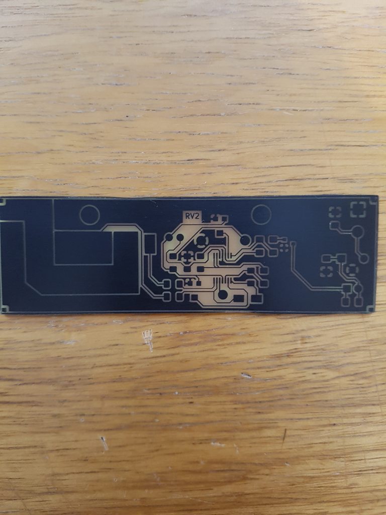
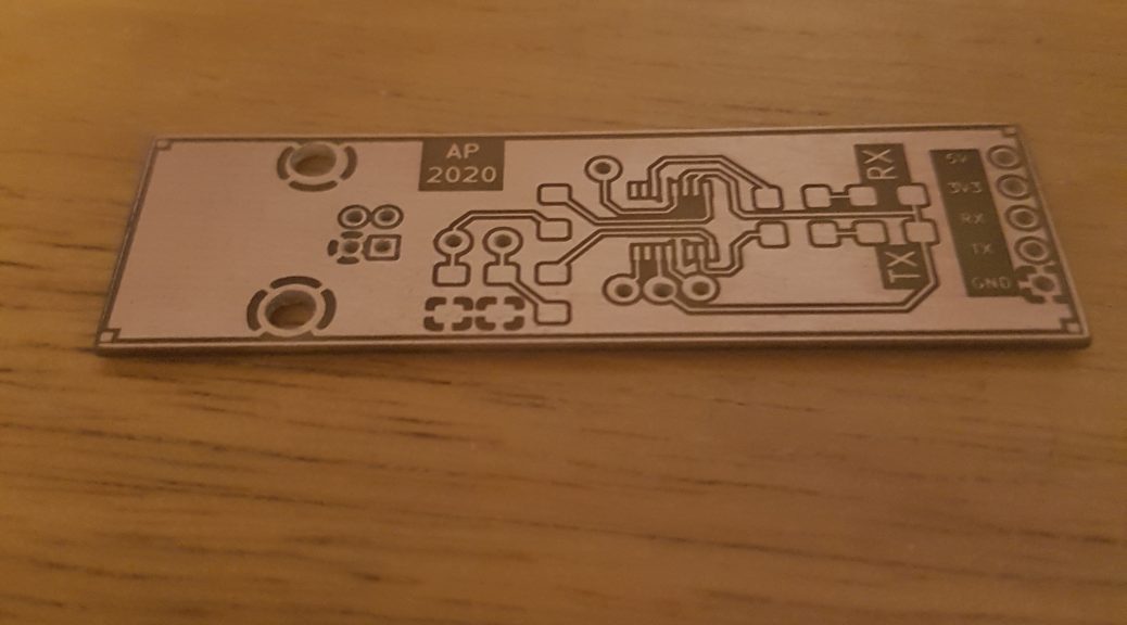
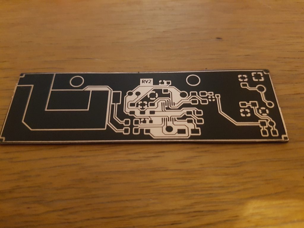
I will share some more results in the next article of this series. Stay tuned if you’re interested!